Update: the DrTm results were for a 6-node cluster, not a 60-node cluster.
Update: corrected the RAM Cloud tpmC number – previously missing a crucial ‘K’ !
The combined changes in networking, memory, storage, and processors that are heading towards our data centers will bring about profound changes to the way we design and build distributed systems, and our understanding of what is possible. Today I’d like to take a moment to summarise what we’ve been learning over the past few weeks and months about these advances and their implications.
Let’s start by looking at the hardware making its way into our data centers, and then we’ll try to make sense of all the implications. (It’s tricky keeping up with all the developments across such a broad front, if I got something wrong or missed something important, please let me know in the comments and I’ll update this post so that everyone can benefit).
Networking
From 10Gbs networking, we’re moving towards the rollout of 40Gbs and 100Gbs ethernet (100GbE). There’s even an IEEE task force working on 400GbE! This gives us very high bandwidth communication in the data center.
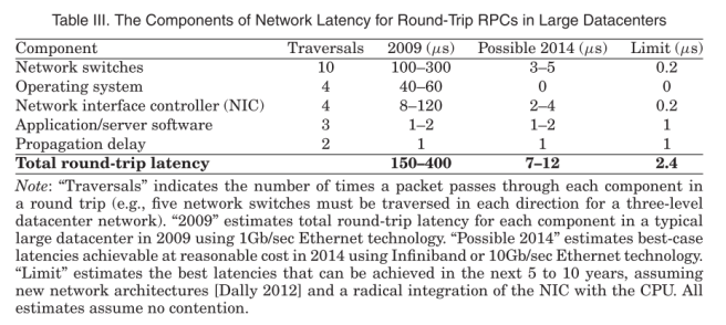
For many distributed applications, we also care very much about latency. Earlier this week we looked at the RAMCloud project which is designing for ultra-low latency. There we find estimates that with a 1GbE network circa. 2009, round-trip RPC latency in a large data center was on the order of 150-400µs. With commonly deployed 10GbE networks in 2014, that number comes down to 7-12µs, the RAMCloud team believe the round-trip latency limit in large data centers will be somewhere around the 2.4µs mark.
Beyond the bandwidth and latency improvements, there’s one other very significant development here: kernel/CPU bypass, in which the network adaptor (NIC) can directly transfer data to or from application memory without involving the CPU at all (so no context switching either). An RPC obviously involves the application server doing some work, but directly reading/writing remote memory with CPU bypass could be achieved with round trip times on the order of 1.4µs!
The technology that enables this is called RDMA (Remote Direct Memory Access). RDMA was originally associated with InfiniBand, but a development called RoCE (RDMA Over Converged Ethernet) supports remote direct memory access over Ethernet. (There’s also iWARP which supports RDMA over TCP/IP, but is not capable of achieving the same level of performance).
RDMA has three modes of communication, from fastest to slowest these are:
- One-sided RDMA (CPU bypass) which provides read, write, and two atomic operations fetch_and_add, and compare_and_swap.
- An MPI interface with SEND/RECV verbs, and
- An IP emulation mode that enables socket-based code to be used unmodified
One-sided RDMA therefore gives us a two order-of-magnitude latency improvement over the round-trip RPC time from currently deployed 10GbE networks, and greatly reduces (i.e., eliminates) CPU overhead.
Main Memory
There are two directions of interest when it comes to main memory, both go under the name NVRAM (Non-volatile RAM), also known as ‘Storage Class Memory’ (SCM). The first direction enables us to treat existing DRAM as if it were non-volatile, and then we have a new generation of NVRAM on its way. It’s a real acronym soup here.
So how do you make existing DRAM non-volatile? You give it just enough back-up power to be able to move data onto non-volatile storage (NAND Flash) in the event of loss of power. That could be via a battery (Battery Back-Up, BBU) or a super-capacitor. One option is to package this inside a DIMM that is plug-replaceable with existing memory – you just put the DRAM plus enough flash to back it up onto the same DIMM. Another option inside the datacenter is to integrate Lithium-ion batteries into the power supply units (PSUs) of each chassis in a rack. This forms a distributed UPS solution and saves memory to commodity SSDs in the event of a primary power failure. This solution can be much more cost effective than NVDIMMs.
Using the distributed UPS approach, it costs approximately an extra 15% over the base cost of the DRAM to be able to treat it as non-volatile.
The new generation of NVRAM technologies can be used as main memory and also as embedded (or even external) storage. We’ll cover the embedded storage use case in the next section. There are a lot of these technologies under development including 3D XPoint, MRAM, MeRAM, Memristor, NRAM, STT-RAM, PCM, CBRAM, RRAM, Millipede, and Racetrack (Better Memory, CACM Jan 2016). 3D XPoint for example, is ~1000x faster than NAND flash storage (your SSD). It doesn’t wear out like flash, and it’s 10x denser than conventional memory. Compared to DRAM it’s cheaper and higher capacity, but slower (exactly how much slower seems hard to find out, somewhere between 10x slower and ‘close to DRAM’ from various sources). Other new NVRAM technologies such as memristors and MeRAM also have 10-1000x greater energy efficiency. When 3D XPoint is used in DIMMs as main memory, the current projection is that a two-socket Xeon server will be able to address up to 6TB of persistent main memory at about half the cost of DRAM.
This chart from Intel (source: Tom’s Hardware) nicely illustrates the blurring of memory and storage capabilities.

Storage
The same NVRAM technology can also be used as embedded or secondary storage.
The PCI Express (PCIe) interconnect means high bandwidth and low latency access to I/O devices. The current generation 3 supports transfer rates of 16GB/s in a 16-lane slot. The forthcoming PCIe 4.0 standard will provide up to 32GB/s of bandwidth in a 16-lane slot, and is currently rumoured to be with us some time in 2017. PCIe is what connects your graphics card to your CPU for example.
NVMe (NVM Express) is a specification for accessing non-volatile memory via the PCIe bus. You can use this to attach NAND flash, or the 1,000x faster new generation of NVM – it was designed with these future technologies in mind. NVMe devices can support hundreds of thousands to millions of IOPS
Here’s Intel’s take on NVMe vs SAS/SATA with 3D XPoint vs NAND Flash:

We can go one step further and put NVMe together with RDMA, resulting in ‘NVMe over Fabrics.’ This allows a client direct access to remote NVRAM, reducing latency and offloading work from the CPU. There is no drop in throughput for NVMe over RDMA compared to NVMe over PCIe, and the latency increase is modest too (from 11/12 µs for 4K random read/write to 18/9µs in one demonstration).
Processing
We’ve become used to GPUs alongside CPUs. This year Intel will start shipping Xeon chips with integrated Field Programmable Gate Arrays (FPGAs). FPGAs can help accelerate tasks such as machine learning and data analytics in an energy efficient way. Previously FPGAs have been linked to the processor via PCIe, putting them onto a dual-chip package means the CPU and FPGA can talk over Intel’s QPI interconnect which is even faster and will allow direct access to Xeon’s on-chip cache and main memory, reducing latency. These will be avaliable on AWS EC2 as well, as ‘C4’ instances.
Next up to I want to highlight hardware transactional memory (HTM) instruction support, available in the x86 instruction set architecture since Haswell as the “Transactional Synchronization Extensions.” It comes in two flavours, a backwards-compatible Hardware Lock Elison (HLE) instruction set, and a more flexible forward-looking Restricted Transactional Memory (RTM) instruction set.
Finally, as we saw yesterday, new persistent memory support is coming to give more control over flushing data from volatile cache into persistent memory.
The New Numbers To Know
This is what looks to be achievable in a data center of the near future. The more I research, the more confusing all the various reports (especially around 3D XPoint) seem to get – many of them appear to conflict with each other. These are my best current guesses, sources are in the notes below. NVRAM’ in the table stands for the next generation of NVRAM, as represented by 3D XPoint. SSD means NAND flash. I would be very grateful for any corrections from those who monitor hardware developments much more closely than I do! Remember that NVRAM’ is just at the beginning of its development curve, so we should expect it to improve rapidly.
                 Latency  Bandwidth  Capacity / IOPS
Register (1)     0.25ns
L1 cache (1)     1ns
L2 cache (1)     3ns
L3 cache (1,2)   11ns                45MB
DRAM    (1,2)    62ns     102GBs     6TB - 4 sockets
NVRAM' DIMM (3)  620ns    60GBs      24TB - 4 socket
1-sided RDMA(4)  1.4us    100GbE     ~700K IOPS
RPC (4)          2.4us    100GbE     ~400K IOPS
NVRAM' NVMe(5,6) 12us     6GBs       16TB/disk, ~2M/600K IOPS 4K Random RW
NVRAM' NVMf(6)   19us     6GBs       16TB/disk, ~700K/600K IOPS 4K Random RW
SSD NVMe (5,7,8) 90us     5GBs       16TB/disk, 850K/150K 4K Random R/W
SSD NVMf (9)     100us    5GBs       16TB/disk, 850K/150K 4K Randow R/W
SAS/SATA SSD (10)110us    1.5GBs     16TB/disk, 200K IOPS
SAS/SATA HDD (10)10ms     1.5GBs     10TB/disk, 200 IOPS
- (Assuming 4GHz Skylake CPU
- Intel Xeon E7
- 3D XPoint will have 8-10x the density of DRAM, but only 4x the capacity. Initial release in NVDIMM DDR4 format will support up to 6TB memory in a two-socket machine (that’s 2x the E7 line on a per-socket basis). I’ve gone with a guess that 4x capacity will be with us before too long. Latency number assumes 10x DRAM (other reports have 2.5x – all quoting Intel!). Bandwidth assumes 60% of DRAM number.
- Limit of what is possible in large scale data center, via RAMCloud paper.
- Latency number from Intel NVMe with 3D XPoint Technology chart (via Tom’s Hardware). Capacity is the same as NAND flash (see (8)). Bandwidth for initial release of 3D XPoint SSD is 6GBs, PCIe 3 x16 could in theory go to 16GBs. IOPS obtained by multiplying SSD DDC P3700 x5, my guess based on Intel IDF figures.
- Microsemi Flash Memory Summit demonstration. Bandwidth in NVMf case upper bound would be capped by network rather than PCE 3 x16, at approx 12GBs (initial release 6GBs). IOPS bound by network?
- Bandwidth & IOPS from Intel SSD DC P3608
- Samsung released a 16TB SSD last year. I’m assuming capacity of the faster SSDs will increase to this kind of size.
- I derived this latency number by adding the extra 10µs of latency to the NVMe numbers.
- Latency from from Intel NVMe with 3D XPoint Technology chart (via Tom’s Hardware). IOPS from wikipedia (SSD at ~1000x HDD). Bandwidth stalls at ~1.5Gbs.
And of course, you can package up multiple disks into storage arrays to increase capacity and IOPS…
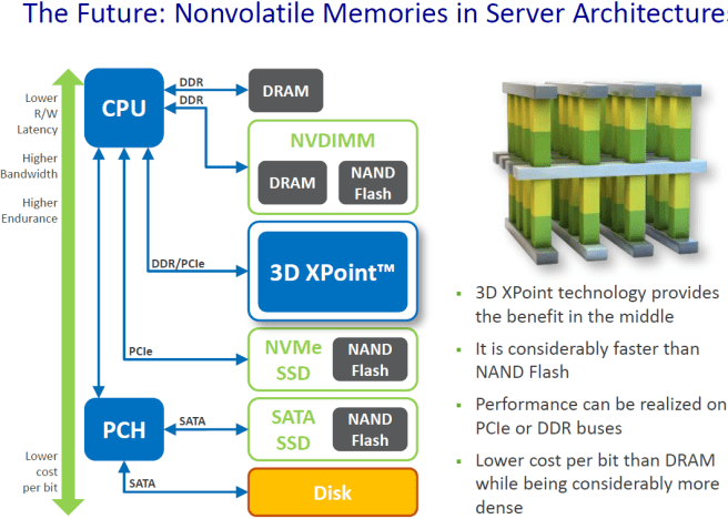
Here’s a handy visual of the various ways non-volatile memories can be used in server architectures (via KitGuru):
Implications for Distributed Systems and Data Stores
A Human Analogy
Let’s try to get an intuition for the change by putting things onto a human scale. Recall the time before digital computers, when computing was a job done by a person. Consider such a human computer sat at their desk doing calculations. Any file on their desk (be it right in front of them, or buried in a pile) can be accessed in about 10 seconds on average. (Files on the desk represents data in registers through L3 cache in this analogy).
If the computer did not have the file they needed already on their desk, then the next best hope was that it could be retrieved from one of the filing cabinets in the office where they worked. Filing was pretty efficient, and any file in a local filing cabinet could be retrieved in about 1 minute. (This represents fetching from memory).
If the file was not present on site in a filing cabinet, then it needed to be retrieved from the warehouse. Oh dear. A trip to the warehouse and back took about 116 days. Worse still, some clients didn’t consider a request completed until the results were safely stored in the warehouse – so they had to wait 116 days for confirmation too. You bet those computers did everything they could to be as efficient as possible with warehouse requests and preferred to do much more local computing than strictly necessary if it meant cutting down on warehouse trips.
File on Desk                    10s
Local Filing Cabinet (Memory)   1 minute
Warehouse (HDD)                 116 days
This is the world the first generation of database systems where designed for.
Along came a new generation of ‘memory’ technology: smarter filing cabinets could store four times as much information, and still let computers get what they wanted within 2-10 minutes. Better still, these improved filing cabinets were fireproof, so clients now considered a request to be completed safely as soon as the results were in a local filing cabinet. 2 minutes vs 116 days was transformative for their business. This had a huge impact on office productivity as you can imagine.
Even more impactful was a new generation of warehouses: SSD warehouses cut file retrieval time from 116 days to about 30hrs, and new-fangled NVMe 3D XPoint warehouses further reduced that to about 3.3hrs. To make the most of all these wonderful developments and exploit the new warehouses to their full capacity, many more computers had to hired.
Offices also had telephones installed so that they could talk to each other. A simple request to read a file that another office had in their filing cabinets could now be satisfied in about 23 minutes, if the remote office needed to do a little more work to satisfy the request, it would take about 40 minutes.
The optimum balance of resources and associated working practices almost certainly look different when any file you want is no more than 3.3 hrs away (vs 116 days), and often much less than that.
File on Desk                  10 secs
Local Filing Cabinet (Memory) 1 minute
Phone another office (RDMA)   23-40 minutes
Warehouse (NVMe)              3 hours 20 minutes
(On this scale, an SSD based warehouse takes about 30 hours).
Research Results
It’s the combination of all these changes at once that lead to so many interesting new systems. A cluster of 10,000 nodes in a large data center could have on the order of 100PB of persistent in-memory data. The RAMCloud key-value store demonstrates read latencies of 5µs and write latencies of 13.5µs at that scale when using RDMA. Using their Reusable Infrastructure for Linearizability the RAMCloud team built a multi-entity distributed transaction mechanism on top of RAMCloud that completed 5-object transactions in about 27µs, and simple distributed transactions execute in about 20µs. At this very low latency, RAMCloud does about 2M transactions per minute (33Ktps) on the TPC-C benchmark in a 10-node cluster.
FaRM exploits persistent memory and RDMA, and demonstrated 4.5M tps in a 90-node cluster on the TPC-C benchmark with 1.9ms of latency at the 99th percentile. The FaRM key-value store clocked 6.3 million operations per second per-machine, with latency at peak throughput of 41µs.
One issue that comes up is understanding when to use 1-side RDMA, and when to use RPCs. In terms of latency, if you need two or more one-sided RDMA calls, then its faster to make one RPC call instead. But one-sided RDMA can bypass the remote CPU, whereas an RPC cannot.
The DrTm system supports distributed transactions combining HTM and RDMA. In a 6-node cluster DrTM achieved 5.5M tps on the TPC-C benchmark. And of course, in-memory transactions are even more interesting if your memory is persistent.
From ARIES to MARS gives a nice example of rethinking transaction and recovery protocols when short random accesses are perfectly acceptable – as the ARIES to MARS authors claim for the new generation of fast NVM – vs designing for long sequential reads. Will append-only techniques be supplanted by update-in-place for example? Will ample persistent memory change persistent formats?
Yesterday in Blurred Persistence we learned of the new implications for the volatile/stable storage boundary between the CPU cache and main memory (when an L3 cache can hold 40+MB of data, that’s still a lot of volatile data) and the new instructions that will be coming to help us manage this.
In Non-volatile Storage we learned of the needs to re-balance systems ensuring enough processing power is available to saturate new storage-class memory devices.
Of course, cost is still going to be a big factor, and we’ll need some updates to the 5-minute rule to take into account new generation NVRAM as cheaper than DRAM, but more expensive than NAND. Power consumption will factor into costs too as some of the new generation NVRAM is much more energy efficient.
Most of these research projects combine one or two of new developments. What happens when you combine fast RDMA networks with ample persistent memory, hardware transactions, enhanced cache management support and super-fast storage arrays? It’s a whole new set of design trade-offs that will impact the OS, file systems, data stores, stream processing, graph processing, deep learning and more. And this is before we’ve even introduced integration with on-board FPGAs, and advances in GPUs…
From a developer perspective, I’m hoping for simpler, safer programming models (the return of distributed transactions for example) for many of today’s use cases. But you can be sure that with all this new power to hand, a whole new set of use cases will emerge to continue pushing at the boundaries of what’s possible.
One for the Berkeley NextLab?
The Berkeley AMPLab that has produced so much wonderful work is now in its final year, and the team are working on plans for what to do next (‘Looking Back at AMP Year 5‘). If ever there was a topic area that seemed ripe for the Berkeley approach to building research centers this is it: cross-discipline, center-wide prototype, lots of collaboration, high-impact – yes please!

Correction: DrTM was evaluated on a 6-node cluster, not a 60-node cluster.