Apps with hardware: enabling run-time architectural customization in smart phones Coughlin et al., USENIX ATC’16
This week we’ve had a couple of hardware-related papers, and one touching on mobile apps (in the context of DNNs). Today’s choice brings those themes together with some really creative thinking – programmable hardware for smartphones! With thanks to Afshaan Mir (@AfshaanMir123) who pointed this paper out to me via Twitter.
Last year AWS gave us F1 instances: EC2 instances with programmable hardware via FPGA (Field Programmable Gate Arrays). You can get up to eight FGPAs in a single F1 instance. If the cloud can do it, why not your mobile phone?! In “Apps with hardware,” Coughlin et al. show us how the inclusion of an FPGA into a smartphone enables mobile apps that include both software and hardware components. Making that work across a range of devices, and enabling multiple apps with hardware to be co-resident presents a few challenges of course, and we’ll look at those shortly. But first, let’s see why on earth anyone might want to do this in the first place!
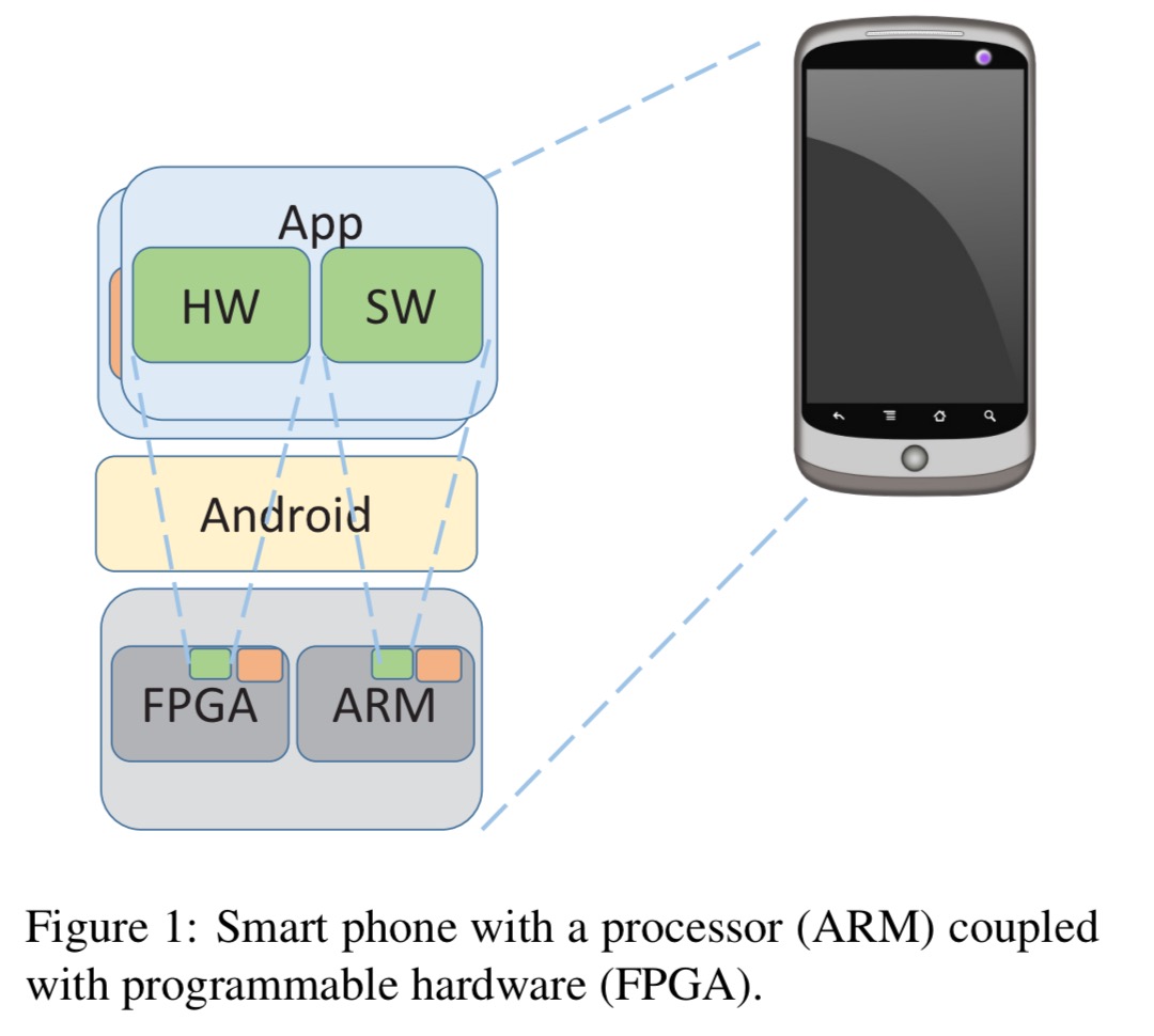
What could you do with a FGPA-equipped phone?
- Build rootkit detection solutions that are independent of the processor and operating system
- Write small hardware co-processors that enable the main processor to enter power saving states more often
- Implement software-defined radio applications
- Accelerate cryptographic operations
- Improve common analytic functions (“One recent example used an FPGA based server to implement common functions used in analytics, and in each case demonstrated that it would require 100-200 servers running Spark to match the performance“.)
- And anything else your imagination can come up with?
Another reason this becomes interesting is that…
… the argument that FPGAs are hard to design for, and therefore not accessible to software app developers, is quickly becoming invalid.
The high-level synthesis (HLS) approach allows developers to use a high-level language such as C or C++ to describe hardware modules.
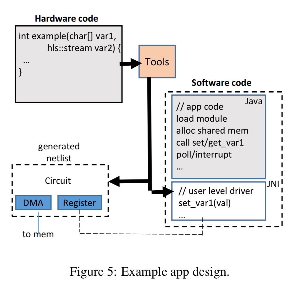
An Android Java app uses the user-level driver app generated by the FPGA vendor’s HLS tool to interface with the hardware module.
Sharing an FPGA across multiple apps
We want the OS to be able to use some of the programmable fabric, in addition to multiple apps which may be installed over time.
The core concept required is run-time reconfiguration, or the ability to dynamically change the FPGA’s configuration (completely or partially) at run-time while it is still operating.
Changing configuration requires a complex mapping of resources. The reconfiguration mechanism supported by vendors (Aletera and Xilinx) comes with many restrictions: “the modules can only work with a single design (in our case, they wouldn’t work across phone architectures), and they can only be loaded in a single location. These restrictions make partial reconfiguration unusable in its current form to enable apps with hardware.”
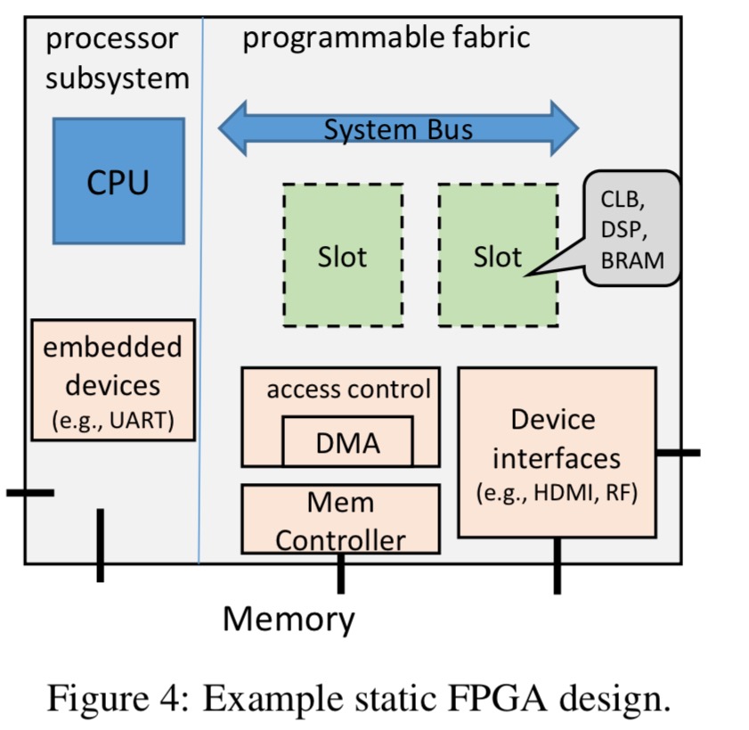
The reconfiguration problem can be simplified by reserving a series of slots – empty and identical areas in the static design. Reconfigurable modules designed to fit within a slot can be created independently.
These areas, or slots, are analogous to PCI slots on a motherboard, where any card can be plugged in independent of the processor. In this case, the ‘cards’ are partial bitstreams (a binary file used to configure and FPGA).
There are still some major challenges though. Partial bitstreams need to be relocatable, which is ok for the logic, but tricky when it comes to enabling static and reconfigurable portions to communicate (“there need to be wires that cross the boundaries, which, in turn, need to be identical for each slot.”) We also need to avoid conflicts between the partial bitstreams and the static design of the main system. All told, this puts a lots of constraints on the static design, to the point of becoming impractical.
The authors solve this puzzle by fitting the partial modules together with a combined compilation step.
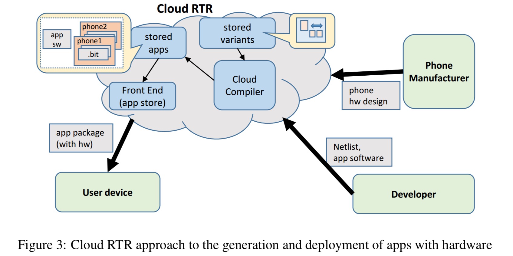
The key idea to enable this is that by leveraging the delivery model of mobile apps (i.e., via an app store), we can effectively merge the modules into various static designs in the cloud, before delivery to the end user. We call this Cloud RTR (RTR for run-time reconfiguration). As illustrated in Figure 3 (below), each phone manufacturer and app developer would submit their design to the Cloud RTR system, and the Cloud RTR system would perform a compilation step to enable a general run-time reconfiguration mechanism.
The design of the phone should allow the reconfigurable modules to interface with the rest of the system resources. A system bus enables slots to communicate with the processor, and a direct memory access (DMA) controller provides access to system memory.
In our approach, we abstract away the ultimate target such that app developers can develop reconfigurable modules that can be loaded onto a variety of platforms. Of note, the reconfigurable modules in our approach can (i) work with multiple slot sizes, (ii) work with multiple slot signaling interfaces, and (iii) be targeted at various end-systems.
App store extensions
The cloud run-time reconfiguration mechanism needs to be integrated into the app store. Vendor tools are set up so that a partial reconfigurable design flow can only be used for a specific static design and target FPGA, and for a specific location within that static design.
Working within that, the Cloud RTR compiler will simply use the vendor tools to compile the module for every static design variant and for every slot within each variant.
The app store ends up storing a data structure that looks something like this:

When an app is downloaded, the app store repackages it with the set of device-specific bitstreams that match the user’s device. For an example app used in the evaluation, the hardware module bitstream came in at 904KB, versus the software component of the app at 5.5MB.
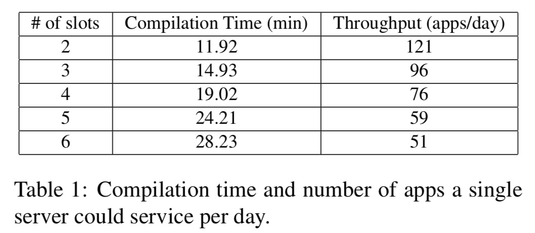
How expensive is all of this in-cloud compilation? The following table shows how long it takes a single server (Intel Xenon CPU) to compile a single app’s reconfigurable module for designs with two to six slots:
If we scale that up to consider an estimated 178K apps uploaded into the Google app store in the month of Jan 2016, then depending on the percentage of those apps that include hardware, the following table shows us the size of compiler farm we need:
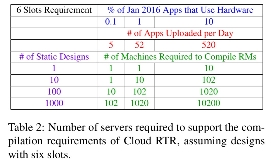
The cloud provider will easily be able to support the lower end of the spectrum internally. On the upper end, the cloud provider might look to relieve the computation burden by offloading to the phone manufacturers to compile for their own variants.
Secure loading
On device, the operating system has access to a secure loading system that can take hardware modules compiled using the Cloud RTR system and load them into the FPGA. If there is an empty slot available, the service will select the compiled module for that slot and load it. If there are no slots available, the OS can create virtual slots by time-slicing existing slots. Context switching takes about 100ms for a 4MB static bitstream, or 27ms for a 1MB hardware model.
Our secure loading mechanism is an extension of secure boot technology where (i) we disable the processor’s connection to the configuration ports of the FPGA, and (ii) we add a module within the static design to support loading of app hardware.
It provides the following guarantees:
- Modules will only be loaded into the slots they are intended for, and cannot overwrite any static configuration
- Code in the OS cannot load a module in a slot which gets access to system memory
- Code in the OS cannot overwrite or unload a trusted module (so that e.g. rootkits can’t unload security modules meant to detect them).
Evaluation
For the experiments, the authors used a prototype mobile device based on a Zedboard development board with integrated Xilinx Zynq 7020 FGPA with embedded dual-core ARM Cortex-A9 CPU, and the Android operating system.
Here are the results for the obligatory AES encryption use case:
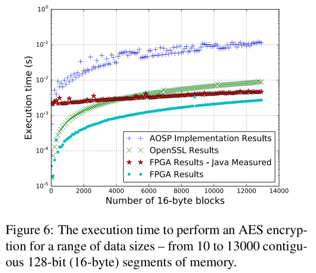
The ‘FPGA – Java Measured’ line shows the actual performance achieved, which includes significant JNI overhead (compare to the pure FPGA line). Even so,
The FPGA implementation is on average three times faster than the OpenSSL implementation, and is approximately 12 times faster than the AOSP.
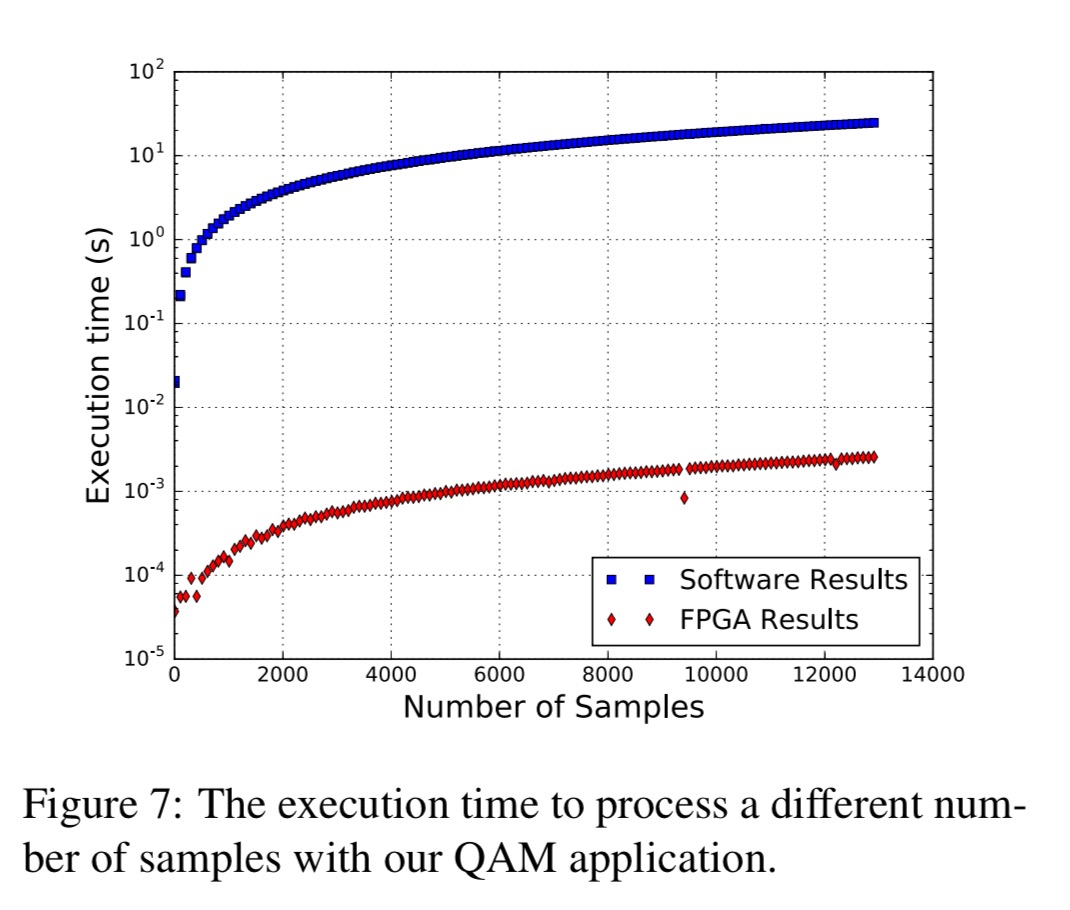
A software-defined radio application processing signal samples achieved an average throughput of 5 Msps (mega-samples per second), while the software implementation only achieves 500 samples/second.
A hardware memory scanner was able to scan memory while the device was in normal operation, with only a 2.7% reduction in read performance, and 5.5% for write operations.
I’ll leave you with this concluding thought from the authors:
There is a great deal of possible future work.
;)
Thanks for writing this post, Adrian. It was only yesterday when I suggested that this “Apps with hardware” paper is very similar to yesterday’s Neurosurgeon, and you have finished reviewing it in no time. Honestly, great work and many thanks !!
I confess I had a head start on the paper before you sent me the link – my turnaround time is a little longer than a day! But many thanks for pointing me at the paper as so often I find good things via referrals like this, which I haven’t already seen.